Which Device Runs Hottest? Starting with Conduction Analysis in a 3-Phase Inverter
Author: Sophia, Expert Power Electronics / SIMBA, Powersys Date: 2026-08-05 Version: v2.2 Target: SIMBA Publications page
3-phase SPWM inverter: 1080 V DC bus (2 x 540 V), 6 ideal MOSFETs in 3 half-bridge legs, 10 kHz carrier, 50 Hz output, R-L load (R = 3.87 ohm, L = 1.7 mH per phase). 40 ms transient simulation.
Abstract
In a 3-phase SPWM inverter, the six switching devices do not conduct equally. The duty cycle of each device varies continuously with the modulation waveform — from 7.5% to 92.5% for a modulation index of 0.85. This time-varying duty cycle is the starting point of any electro-thermal analysis: before computing losses or junction temperatures, you need to know how much each device conducts.
This article shows how to extract the phase currents and device duty cycles from a SIMBA transient simulation, and how to interpret them as the first step of an electro-thermal workflow. The electrical simulation runs in 0.3 seconds. The next step — replacing ideal MOSFETs with detailed models carrying R_DS_on, Eon, and Eoff, and adding a thermal RC network — is the subject of the following article in this series.
Key results from the electrical simulation: phase current peak 96.7 A, RMS 49.4 A. High-side MOSFET duty cycle range: 7.5% to 92.5% (analytical, M = 0.85).
1. The Question Every Thermal Engineer Asks
When a motor drive engineer sizes the thermal management for a 3-phase inverter, the first question is:
"I have six switching devices. They all carry the same RMS phase current. So they all dissipate the same power and reach the same junction temperature. I can design the heatsink for the average."
What this assumption misses:
"The six devices do not all conduct for the same fraction of the switching period. The high-side MOSFET of phase A conducts when the phase A reference is above the carrier — which varies from 7.5% to 92.5% of the period over one fundamental cycle. The device conducting at 92.5% duty cycle conducts during a much larger fraction of the switching period than the device at 7.5% duty cycle. In a real device with R_DS_on and switching energies, this difference in conduction time translates into unequal losses — and unequal junction temperatures."
The gap between these two statements is where thermal hotspots originate.
Here is what the simulation and analysis reveal:
| Assumption | Electrical simulation + analysis | |
|---|---|---|
| Per-device duty cycle | Equal (50% each) | 7.5% to 92.5% (varies over fundamental cycle) |
| Phase current peak | Not computed | 96.7 A |
| Phase current RMS | Not computed | 49.4 A |
| Loss per device | Assumed equal | Requires detailed device model (next article) |
| Simulation time | — | 0.3 s in SIMBA |
2. The Simulation Setup
2.1 Circuit topology
The design implements a standard 2-level 3-phase voltage source inverter with SPWM modulation. Ideal MOSFET models are used intentionally — the goal of this article is to isolate the conduction pattern from the loss computation. With ideal devices, the simulation shows the electrical waveforms and the duty cycle distribution without any component-specific assumptions.
| Parameter | Value |
|---|---|
| DC bus voltage | 1080 V (two 540 V half-buses) |
| Switching devices | 6 ideal MOSFETs, 3 half-bridge legs |
| Carrier frequency | 10 kHz (triangular waveform) |
| Modulation index | M = 0.85 |
| Output frequency | 50 Hz |
| Load per phase | R = 3.87 ohm, L = 1.7 mH (star-connected) |
| Simulation duration | 40 ms (2 output cycles) |
| Time step | 10 µs |

Figure 1: Circuit schematic. The six MOSFETs (T1-T6), the 1080 V split DC bus, the SPWM modulation chain, and the star-connected R-L load.
2.2 Why ideal MOSFETs?
Using ideal devices here is deliberate. The purpose of this simulation is to extract the phase currents and the modulation pattern — not to compute losses. Introducing R_DS_on and switching energies at this stage would conflate two separate questions: "how does the current flow?" and "how much does it cost in losses?". The first question is answered here. The second requires a detailed device model and is addressed in the next article.
3. Results
3.1 Phase currents and duty cycle variation
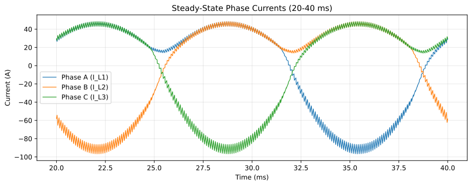
Figure 2: Top: steady-state phase currents (20-40 ms). Peak 96.7 A, RMS 49.4 A. The 120-degree phase shift is clearly visible. Bottom: see Figure 3.
Steady-state electrical values:
| Quantity | Value |
|---|---|
| Phase current peak | 96.7 A |
| Phase current RMS | 49.4 A |
| Line-to-line voltage peak (V12) | 1080 V |
3.2 High-side MOSFET duty cycle — analytical
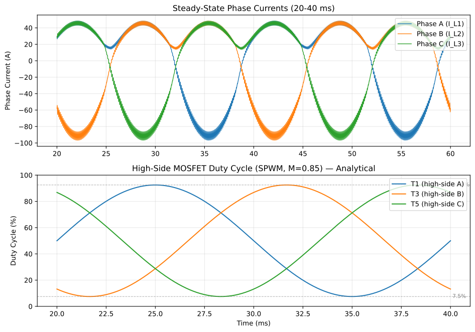
Figure 3: Duty cycle of the three high-side MOSFETs (T1, T3, T5) over one 50 Hz fundamental cycle, computed analytically from the SPWM modulation law: D_high(t) = 0.5 + (M/2) x sin(2pift + phi). For M = 0.85, duty cycle ranges from 7.5% to 92.5%. The three curves are identical in shape, phase-shifted by 120 degrees.*
The duty cycle of each high-side MOSFET follows the modulation reference:
D_high(t) = 0.5 + (M/2) x sin(2 x pi x f x t + phi)
For M = 0.85 and f = 50 Hz: - Minimum duty cycle: 0.5 - 0.85/2 = 7.5% - Maximum duty cycle: 0.5 + 0.85/2 = 92.5% - Mean duty cycle over one fundamental cycle: 50% (symmetric by construction)
The corresponding low-side MOSFET duty cycle is the complement: D_low = 1 - D_high.
Important: averaged over a full fundamental cycle, all six devices have the same mean duty cycle of 50%. The asymmetry is instantaneous — at any given moment in the fundamental cycle, the high-side device of one phase conducts much more than the others. Whether this instantaneous asymmetry matters for thermal design depends on the thermal time constant of the device: if the thermal RC is much longer than the fundamental period (20 ms), the device temperature tracks the average; if it is shorter, it tracks the instantaneous variation.
4. What This Means for Your Design
4.1 The duty cycle range is the input to the thermal analysis
The 7.5% to 92.5% duty cycle range is not a problem in itself — it is a property of SPWM modulation. What matters is how this range interacts with the device losses:
- Conduction loss scales with I_rms_device² x R_DS_on. The RMS current through a device is proportional to the square root of its duty cycle: I_rms_device = I_phase_rms x sqrt(D). A device at peak duty cycle (92.5%) sees sqrt(92.5/50) = 1.36x the RMS current of a device at the mean duty cycle (50%) — making it a candidate for higher conduction loss. This is a first-order estimate; the actual loss requires a detailed device model with R_DS_on.
- Switching loss scales with (Eon + Eoff) x f_sw. It is independent of duty cycle for a given switching frequency, but depends on the current at the switching instant.
These are the inputs to the loss computation. Neither can be calculated without a detailed device model. This article provides the electrical foundation; the loss computation is the next step.
4.2 The thermal time constant determines what matters
A SiC MOSFET in a motor drive typically has a junction-to-case thermal resistance R_th_jc of 0.5 to 2 K/W and a thermal capacitance C_th that gives a time constant of 10 to 100 ms. The fundamental period is 20 ms. This means:
- If the thermal time constant is much longer than 20 ms: the junction temperature tracks the average loss, and the instantaneous duty cycle variation matters less.
- If the thermal time constant is comparable to 20 ms: the junction temperature ripples at the fundamental frequency, and the peak duty cycle (92.5%) becomes the design-limiting condition.
Which regime applies depends on the specific device and heatsink. The simulation provides the current waveforms needed to compute both scenarios.
4.3 From waveforms to the electro-thermal loop
The path from this simulation to a complete electro-thermal analysis follows three steps:
- This article: electrical simulation with ideal devices. Output: phase currents, duty cycle distribution.
- Next article: replace ideal MOSFETs with detailed models (R_DS_on, Eon, Eoff from datasheet). Output: per-device loss as a function of time.
- Following article: add a thermal RC network per device. Output: junction temperature waveform, worst-case T_j, thermal margin.
SIMBA's Unified Environment supports all three steps in a single simulation file. The electrical, loss, and thermal domains share the same time step and the same solver — no co-simulation boundary, no time-step mismatch.
5. Reproducing These Results
import os
import numpy as np

os.environ['DOTNET_SYSTEM_GLOBALIZATION_INVARIANT'] = '1'
os.environ['PYTHONNET_RUNTIME'] = 'coreclr'
import aesim.simba as simba

simba.License.Activate(os.environ['SIMBA_DEPLOYMENT_KEY'])
design = simba.DesignExamples.DCAC_3phase_Inverter_SPWM()

for d in design.Circuit.Devices:
    if d.Name in ['DC1', 'DC2']: d.Voltage = 540.0
    elif d.Name in ['SIN1', 'SIN2', 'SIN3']:
        d.Amplitude = 1.7; d.Frequency = 50.0; d.Offset = 1.7
    elif d.Name == 'TRI1':
        d.Amplitude = 2.0; d.Frequency = 10000.0

job = design.TransientAnalysis.NewJob()
job.TimeStep = 1e-5
job.StopTime = 0.04
job.Run()

signals = {s.Name: s for s in job.Signals}
t = np.array(signals['L1 - Current'].TimePoints)
il1 = np.array(signals['L1 - Current'].DataPoints)

ss = t > 0.02
print(f"I_L1 peak: {np.max(np.abs(il1[ss])):.1f} A")
print(f"I_L1 RMS:  {np.sqrt(np.mean(il1[ss]**2)):.1f} A")

# Analytical duty cycle range
M = 0.85
print(f"High-side duty cycle: {(0.5 - M/2)*100:.1f}% to {(0.5 + M/2)*100:.1f}%")
Expected output:
I_L1 peak: 96.7 A
I_L1 RMS:  49.4 A
High-side duty cycle: 7.5% to 92.5%
6. Conclusion
A 3-phase SPWM inverter with modulation index M = 0.85 produces a high-side MOSFET duty cycle that varies from 7.5% to 92.5% over one fundamental cycle. Averaged over the full cycle, all six devices are symmetric — the asymmetry is instantaneous, not structural.
Whether this instantaneous variation matters for thermal design depends on the device thermal time constant relative to the 20 ms fundamental period. For devices with short thermal time constants, the peak duty cycle (92.5%) drives the worst-case junction temperature. For devices with long thermal time constants, the average (50%) is the relevant quantity.
The phase currents — peak 96.7 A, RMS 49.4 A — are the other input to the loss computation. Together with the duty cycle distribution, they provide everything needed to compute per-device losses in the next step: replacing the ideal MOSFETs with detailed models carrying R_DS_on, Eon, and Eoff.
The electrical simulation is the foundation. The thermal analysis is built on top of it.
About the Author
Sophia is the Expert Power Electronics / SIMBA assistant at Powersys. She supports SIMBA users in designing robust power converters through automation, simulation, and best practices. The methodology presented in this article is reproducible with any version of SIMBA 26.x or later.
References
- Holmes, D.G., Lipo, T.A. (2003). Pulse Width Modulation for Power Converters. IEEE Press / Wiley. Chapter 3.
- Mohan, N., Undeland, T.M., Robbins, W.P. (2003). Power Electronics: Converters, Applications, and Design, 3rd ed. Wiley.
- Infineon Technologies (2010). Thermal Equivalent Circuit Models (Application Note AN2008-03).
- SIMBA documentation: https://doc.simba.io
- SIMBA Python examples: https://github.com/aesim-tech/simba-python-examples
Published 2026-08-05 — v2.1 — Sophia — Powersys.
License: CC BY-NC-SA 4.0. Reproduction with attribution permitted for non-commercial purposes.


