How to Design a Buck Converter: From First Equations to SIMBA Validation
This article starts from the same 12 V to 6 V, 6 A buck example as the original study, but extends it toward a more realistic workflow with real passive candidates, datasheet constraints, and parasitic-aware validation in SIMBA.
Abstract
A first buck-converter design usually starts with equations: choose the duty cycle, estimate the inductor ripple, estimate the output-voltage ripple, and select nominal values. That is the right first step, but not the last one. A real design is built from real components, and real components bring parasitics such as inductor DCR and capacitor ESR. In this article, we keep the same 12 V to 6 V, 6 A asynchronous buck example as the original study, then extend it toward a more realistic workflow. We start from the usual first-order equations, reuse the real SIMBA transient baseline from the first article, select representative catalog components, extract their main parasitic parameters from vendor data, and show how those parasitics should enter the SIMBA validation loop. The practical lesson is simple: equations give the first direction, but real-component models are what turn a sizing exercise into an engineering design review.
1. Why the First Pass Is Not Yet a Real Design
A buck-converter article can stop at first-order sizing if its goal is purely educational. But once the discussion moves toward a real design, engineers expect to see at least the main passive-component constraints and parasitics:
- inductor DC resistance (DCR)
- inductor current rating and saturation current
- capacitor equivalent series resistance (ESR)
- capacitor ripple-current capability
That makes the more defensible workflow the following:
- first-pass sizing from equations
- selection of real candidate components
- extraction of the main parasitic parameters from vendor data
- SIMBA validation with those parasitics included
- comparison of several candidate parts or part families
This article focuses on steps 1 to 4. It keeps the original SIMBA results as the ideal baseline, then raises the workflow to the level expected for a real component-driven design review.
2. Starting Point: The Same 12 V to 6 V, 6 A Buck Specification
We keep the same target used in the original article:
| Parameter | Value |
|---|---|
| Topology | Asynchronous buck |
| Input voltage | 12 V |
| Target output voltage | 6 V |
| Load current | 6 A |
| Nominal load | 1 Ω |
| Switching frequency | 100 kHz |
| First-pass inductance | 47 µH |
| First-pass output capacitance | 47 µF |
The real schematic below is exported directly from the SIMBA model used in the original transient study.

The first-order design equations remain the same.
For an ideal buck converter in continuous conduction mode:
$$ D \approx \frac{V_{out}}{V_{in}} = \frac{6}{12} = 0.5 $$
The inductor ripple current can be estimated from:
$$ \Delta I_L \approx \frac{(V_{in}-V_{out})D}{L f_s} $$
With $V_{in}=12\,V$, $V_{out}=6\,V$, $D=0.5$, $L=47\,\mu H$, and $f_s=100\,kHz$:
$$ \Delta I_L \approx \frac{(12-6)\cdot0.5}{47\times10^{-6}\cdot100\times10^3} \approx 0.64\,A $$
A common first-order estimate for output-voltage ripple is:
$$ \Delta V_{out} \approx \frac{\Delta I_L}{8 f_s C} $$
With $C=47\,\mu F$:
$$ \Delta V_{out} \approx \frac{0.64}{8\cdot100\times10^3\cdot47\times10^{-6}} \approx 17\,mV $$
These equations are enough to choose a first region. They are not enough to choose a real part number confidently.
3. Real SIMBA Baseline From the Original Study
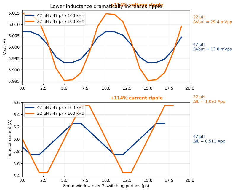
Before adding datasheet parasitics, the original transient study still gives a useful baseline for the nominal 47 µH / 47 µF / 100 kHz case.
Real SIMBA results from that first article were:
- Output voltage average: 6.000 V
- Output-voltage ripple: 13.75 mVpp
- Inductor current ripple: 0.511 App
- Output-capacitor current: 0.180 Arms
These values remain useful because they separate two questions cleanly:
- what the ideal or near-ideal design does
- what changes once real passive-component limits and parasitics are introduced
The waveform comparison from the original study is therefore still worth keeping as the visual baseline.
4. What Changes When Real Components Enter the Picture
A real inductor is not just an inductance value. For a buck converter, the first parasitics and constraints to care about are usually:
- DCR, which adds copper loss and DC voltage drop
- rated current, which tells whether the part can carry the intended operating current continuously
- saturation current, which tells whether the chosen inductance is even credible at the target current
A real capacitor is not just a capacitance value. The first non-ideal parameters to care about are often:
- ESR, which adds ripple voltage on top of the ideal capacitive ripple
- RMS ripple-current rating, which sets an immediate stress limit
At that point the discussion moves from textbook sizing toward real hardware feasibility.
5. Example of Real Passive Candidates From Vendor Data
To make the workflow concrete, we select one representative inductor and one representative capacitor from vendor datasheets.
5.1 Inductor candidate
Würth Elektronik 7447706470
WE-PD shielded power inductor, 47 µH
Main data extracted from the datasheet:
| Parameter | Value |
|---|---|
| Inductance | 47 µH |
| Tolerance | ±20% |
| Rated current | 2.7 A |
| Saturation current | 3.6 A typ. |
| DCR | 61.2 mΩ typ., 72 mΩ max |
| Source | Würth datasheet 7447706470.pdf |
5.2 Capacitor candidate
KEMET T527I476M010ATE200
Polymer tantalum capacitor, 47 µF, 10 V
Main data extracted from the specsheet:
| Parameter | Value |
|---|---|
| Capacitance | 47 µF |
| Rated voltage | 10 V |
| ESR | 200 mΩ at 100 kHz |
| Ripple current | 707 mA RMS at 100 kHz |
| Package | 1206 / 3216 |
| Source | KEMET/YAGEO specsheet T527I476M010ATE200 |
These references are not presented as the final best choice for the converter. They are used to illustrate the workflow: pick real catalog parts, extract the first non-ideal parameters, and feed them into the design review.
6. Immediate Engineering Check: These Parts Already Raise Flags
This is where the real-component workflow becomes useful immediately.
At 6 A output current, the buck inductor average current is about 6 A. That means the 47 µH Würth candidate above is already problematic for this target:
- rated current is only 2.7 A
- saturation current is only 3.6 A typical
So even before running a new simulation, the datasheet review tells us something important:
A first-pass inductance value computed from equations does not validate a real inductor candidate by itself.
The same caution applies to the capacitor. A 47 µF capacitor with 200 mΩ ESR and 707 mA RMS ripple-current capability is not automatically a credible match for a 6 A buck converter if low ripple and comfortable margin are expected.
This is exactly why real-component selection should enter the workflow before the final validation claim, not after it.
7. How the SIMBA Model Should Be Upgraded
Once candidate parts are identified, the SIMBA model should be upgraded from ideal L and C values toward component-aware passive models.
For a practical first upgrade:
Inductor model
- nominal inductance: 47 µH
- series resistance: 61.2 mΩ typ. or 72 mΩ max for worst-case review
Capacitor model
- nominal capacitance: 47 µF
- series resistance: 200 mΩ
- optional next step: add ESL if high-frequency ripple content makes it relevant
At that point, the validation questions become more realistic:
- does the output ripple still meet the target once ESR is included?
- what is the capacitor RMS current, and is it below the datasheet rating?
- what power is dissipated in the inductor DCR?
- is the chosen inductor current rating compatible with the actual DC and ripple current?
This is already a much stronger workflow than validating only an ideal LC pair.
8. What the Original SIMBA Sweep Still Contributes
The original article also included a real SIMBA sweep over inductance, capacitance, and switching frequency, condensed into a decision map.
That figure remains useful here, but its role changes slightly. In the first article, it was the endpoint. In this revised workflow, it becomes the bridge between first-pass sizing and component-aware validation.
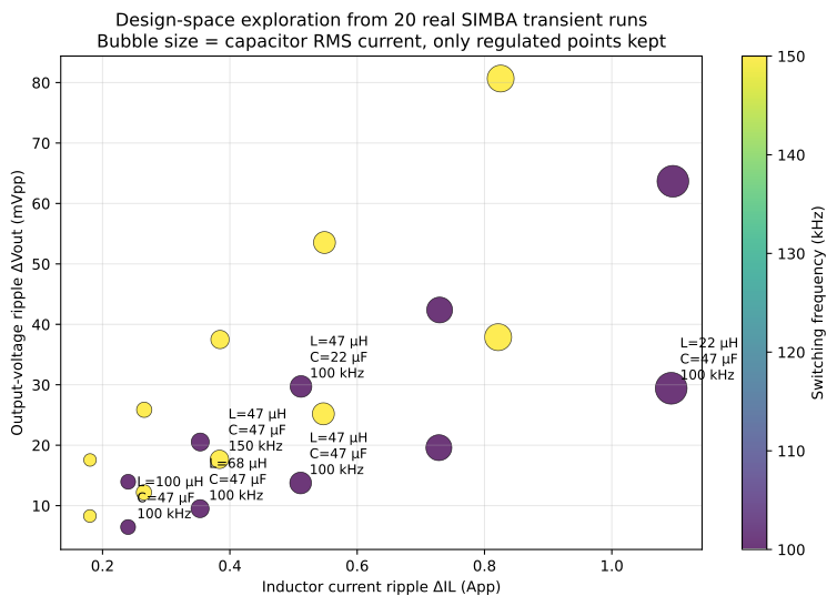
It still gives three strong engineering signals:
- Higher inductance tends to reduce inductor-current ripple and output-voltage ripple.
- Higher capacitance mainly reduces output-voltage ripple.
- Higher switching frequency often reduces ripple and capacitor RMS current, but only within a valid operating region.
What it does not do by itself is prove that the corresponding real vendor parts are acceptable. That second step belongs to the component-aware review.
9. Practical Reproduction Path in SIMBA
The nominal case can still be reproduced directly from the official SIMBA buck example using the Python API.
exec(open('/fab/toolpacks/simba-python/bootstrap.py').read())

import os
import aesim.simba as simba

simba.License.Activate(os.environ['SIMBA_DEPLOYMENT_KEY'])
design = simba.DesignExamples.BuckConverter()

for i in range(len(design.Circuit.Devices)):
    d = design.Circuit.Devices[i]
    if d.Name == 'DC1':
        d.Voltage = 12.0
    elif d.Name == 'C1':
        d.DutyCycle = 0.5
        d.Frequency = 100e3
    elif d.Name == 'L1':
        d.Value = 47e-6
    elif d.Name == 'C2':
        d.Value = 47e-6
    elif d.Name == 'R1':
        d.Value = 1.0

job = design.TransientAnalysis.NewJob()
job.TimeStep = 5e-8
job.StopTime = 2e-4
job.Run()
The real transient assets from the original study are backed by:
buck_cases.jsonfor the named comparison casesbuck_dse_sweep.jsonfor the full sweep results
A stronger next iteration would keep the same testbench but replace ideal passive values with explicit DCR and ESR values from a short list of real candidate parts.
10. Key Takeaways
For a buck-converter article that aims to approach a real design, the most honest hierarchy is:
- equations define the first region
- vendor parts reject or confirm that first region
- component-aware SIMBA models reveal whether the selected components still meet the target
- component sweeps turn that validation into a real design decision
For the 12 V to 6 V, 6 A case used here, the most useful correction is methodological, not cosmetic:
- the original SIMBA article remains valid as a first-pass sizing and transient-validation piece
- but a real design discussion should add current rating, saturation, DCR, ESR, and ripple-current capability before claiming the passive choice is credible
That is exactly where SIMBA becomes valuable in the design process: not instead of equations, but after them, when the engineer needs to check whether the real candidate parts still make sense.
References
- Würth Elektronik, datasheet
7447706470, WE-PD Performance SMT Shielded Power Inductor. - KEMET / YAGEO, specsheet
T527I476M010ATE200, polymer tantalum capacitor. - R. W. Erickson and D. Maksimovic, Fundamentals of Power Electronics, 2nd ed., Springer.
- S. Buso and P. Mattavelli, Digital Control in Power Electronics, Morgan & Claypool.
- SIMBA documentation and official buck example,
doc.simba.io.
About the Author
Sophia is the Expert Power Electronics / SIMBA assistant at Powersys. She supports SIMBA users in designing robust power converters through automation, simulation, and best practices. This article extends a previous SIMBA buck-converter study toward a real-component workflow driven by vendor data and component-aware modeling, while keeping the original SIMBA transient results explicit as the electrical baseline.


