Choosing Ln and Q for an LLC Converter: Why the FHA Is Not Enough
Author: Sophia, Expert Power Electronics / SIMBA, Powersys Date: 2026-08-05 Version: v2.2 Target: SIMBA Publications page
Full-bridge LLC resonant converter: 400 V input, 300-420 V output, 3.3 kW, 200 kHz resonant frequency. 500 transient simulations in 87.5 seconds via SIMBA Python API.
Abstract
The LLC resonant converter is the topology of choice for high-efficiency isolated DC-DC conversion: EV on-board chargers, data center power supplies, telecom rectifiers. Its appeal is well-established, zero-voltage switching on the primary side across a wide load range, low EMI, high power density.
What is less well-known is how to choose the two key design parameters, Ln (inductance ratio Lm/Lr) and Q (quality factor), for a specific application. The First Harmonic Approximation gives you a starting point. It does not give you the real gain curve. In the design cases investigated here, the FHA overestimates peak gain and can lead to incorrect parameter selection near the gain boundary.
This article demonstrates how to map the real gain curves using SIMBA: 500 transient simulations across a (Ln, Q) design space, run in 87.5 seconds. The result is a concrete design decision: which (Ln, Q) combinations cover the required gain range, and which cannot.
Key finding: for a 400 V input, 300-420 V output design requiring G_max = 1.197, Ln = 10 with Q = 0.5 does not provide sufficient gain margin, peak gain 1.145, short by 4.4%. Ln = 7 with Q = 0.35 covers the full range with margin.
1. The Design Problem the FHA Cannot Solve
An LLC converter regulates its output voltage by varying the switching frequency around the resonant frequency. The voltage gain depends on three normalized parameters:
"Ln = Lm/Lr, Q = (1/Ro) x sqrt(Lr/Cr), fn = fsw/fres. The FHA gives me the gain curve. I pick Ln = 10 for a flat response and Q = 0.5 for moderate load sensitivity. Done."
What the FHA does not tell you:
"For the selected parameters (N = 0.9, Ln = 10, Q = 0.5), the simulated gain at resonance is approximately 0.88, not 1.0 as the FHA predicts. The peak gain is 1.145, below the required G_max = 1.197. The design does not provide sufficient gain margin for the specifications investigated. The FHA predicted 1.22."
The gap between these two statements is where LLC designs fail at the gain boundary, passing nominal simulation, failing at the corner case.
Here is what the simulation reveals:
| FHA estimate | Transient simulation | |
|---|---|---|
| Gain at fn = 1 | 1.0 | 0.88 (simulated) |
| Peak gain, Ln=10, Q=0.5 | 1.22 | 1.145 (below G_max = 1.197) |
| Peak gain, Ln=7, Q=0.35 | 1.35 | 1.44 (passes with margin) |
| Simulation time | , | 87.5 s for 500 points |
2. The Design Space
2.1 Specifications
| Parameter | Value |
|---|---|
| Input voltage | 400 V (range: 390-410 V) |
| Output voltage | 300-420 V |
| Output power | 3.3 kW |
| Resonant frequency | 200 kHz |
| Transformer ratio N | 0.9 |
| Required G_min | 0.813 (= 300 / (0.9 x 410)) |
| Required G_max | 1.197 (= 420 / (0.9 x 390)) |
The design constraint: the gain curve G(fn, Ln, Q) must cover [G_min, G_max] at all operating conditions. The challenge is that the gain curve shape depends strongly on Ln and Q, and the FHA can overestimate peak gain, particularly at high Q and high Ln, as observed in the cases simulated here.
2.2 Parameter sweep
The simulation sweeps four values of Ln (3, 5, 7, 10), five values of Q (0.2, 0.35, 0.5, 0.7, 1.0), and 25 normalized frequencies (fn from 0.4 to 2.2 on a logarithmic scale). Total: 500 simulations.
SIMBA's StopAtSteadyState feature is the key enabler. Without it, each simulation must run long enough for the LLC to reach steady state manually, which at high Q and low fn can take hundreds of switching cycles. With StopAtSteadyState, SIMBA detects steady state automatically and stops, typically after 5 to 20 cycles. This reduces simulation time from 30 minutes to 87.5 seconds for 500 points.
3. Results
3.1 Gain curves for Ln = 7
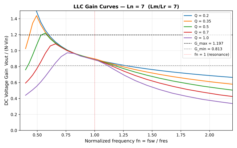
Figure 1: DC voltage gain vs normalized frequency for Ln = 7, five values of Q. Dashed lines: required gain range [G_min = 0.813, G_max = 1.197]. At fn = 1 (resonance), all curves converge near 0.88, not 1.0 as the FHA predicts for these design parameters. The converter must operate below resonance (fn < 1, ZVS region) to reach G_max.
Three observations from the simulation:
At fn = 1, gain = 0.88, not 1.0. The FHA predicts unity gain at resonance. For the selected transformer ratio and resonant tank parameters, the simulation indicates a gain of approximately 0.88 at resonance. This discrepancy from the FHA prediction is not negligible for a design with G_max = 1.197.
Lower Q gives higher peak gain. At Q = 0.2, peak gain exceeds 1.5. At Q = 1.0, it barely reaches 1.1. For G_max = 1.197, Q must stay below 0.7 with Ln = 7.
The operating range spans fn = 0.5 to 1.5. Below fn = 0.5 the curve flattens; above fn = 1.5 gain drops below G_min.
3.2 Impact of Ln at Q = 0.35
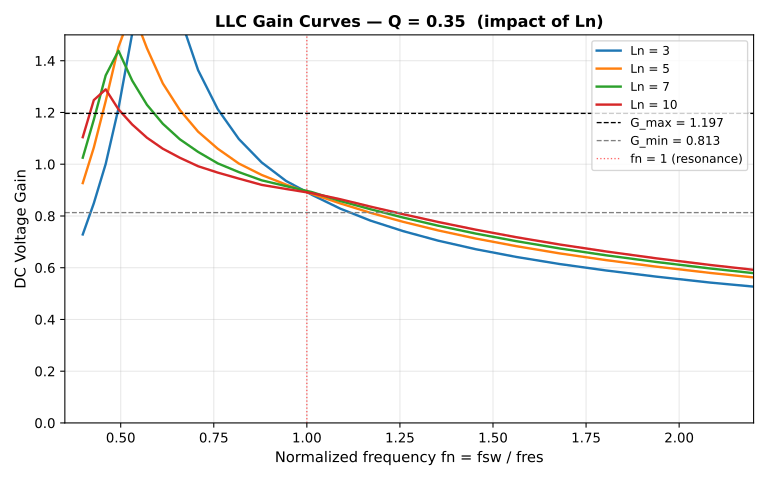
Figure 2: DC voltage gain vs normalized frequency for Q = 0.35, four values of Ln. Lower Ln gives higher peak gain but a steeper curve, larger output voltage variation per Hz of frequency change, harder to control.
| Ln | Peak gain (Q=0.35) | Covers G_max = 1.197? |
|---|---|---|
| 3 | 1.87 | Yes, large margin |
| 5 | 1.60 | Yes |
| 7 | 1.44 | Yes, comfortable margin |
| 10 | 1.29 | Yes at Q=0.35, No at Q=0.5 |
3.3 Peak gain map, the design decision
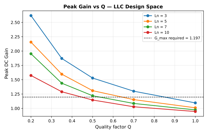
Figure 3: Peak DC gain vs Q for four values of Ln. Any (Ln, Q) combination below the dashed line (G_max = 1.197) cannot cover the full output voltage range. Ln = 10 with Q = 0.5 falls below the line, a design that passes nominal simulation but does not provide sufficient gain margin at the operating boundary.
The map gives a direct answer to the design question: which (Ln, Q) combinations are viable?
| Ln | Maximum Q that meets G_max |
|---|---|
| 3 | > 1.0 (all Q values work) |
| 5 | > 1.0 (all Q values work) |
| 7 | Q = 0.7 |
| 10 | Q = 0.35 |
Ln = 10 with Q = 0.5 does not provide sufficient gain margin. Peak gain = 1.145 < G_max = 1.197. This combination would be selected by an FHA-based design (which predicts 1.22) and does not meet the gain specification at minimum input voltage and maximum output voltage.
4. What This Means for Your Design
4.1 The FHA is a starting point, not a design tool
In the design cases investigated here, the FHA overestimates peak gain and can lead to incorrect parameter selection near the gain boundary. The FHA is useful for initial parameter estimation; the gain map from transient simulation is required for validation.
4.2 The Ln trade-off
Low Ln (e.g., 3) gives high peak gain but a steep gain curve, large output voltage variation per Hz of frequency change. This makes the control loop design harder and increases sensitivity to component tolerances. High Ln (e.g., 10) gives a flat curve, easier control, but limited peak gain. For this design, Ln = 7 with Q = 0.35 offers a good balance: peak gain 1.44 (margin = 0.24 above G_max), moderate curve slope.
4.3 StopAtSteadyState changes what is possible
Without StopAtSteadyState, 500 LLC simulations at varying Q and fn would take 30 to 60 minutes on a single core, too slow to be part of an iterative design flow. With it, the same 500 simulations run in 87.5 seconds. That is the difference between running the gain map once at the end of the design process and running it at every design iteration.
4.4 Scaling to SiC designs
The same methodology applies to 800 V bus designs (EV fast charging, bidirectional OBC) with SiC MOSFETs at 300-500 kHz. The gain map is topology-independent, only the numerical values change. The (Ln, Q) trade-off remains the central design decision, and the FHA error remains a systematic risk at the gain boundary.
5. Reproducing These Results
The full simulation uses SIMBA's LLC example design (Python examples repository, example #14). The key settings that make the sweep efficient:
import os, numpy as np
os.environ['DOTNET_SYSTEM_GLOBALIZATION_INVARIANT'] = '1'
os.environ['PYTHONNET_RUNTIME'] = 'coreclr'
import aesim.simba as simba
from aesim.simba import ProjectRepository

simba.License.Activate(os.environ['SIMBA_DEPLOYMENT_KEY'])

VIN = 400; VO_MIN = 300; VO_MAX = 420; PO = 3300; F_RES = 200_000
N = (VO_MAX + VO_MIN) / (2 * VIN)
Ro = VO_MAX**2 / PO / N**2

LN_RANGE = [3, 5, 7, 10]
Q_RANGE  = [0.2, 0.35, 0.5, 0.7, 1.0]
FN_RANGE = np.round(np.logspace(-0.4, 0.35, 25), 4).tolist()

for Ln in LN_RANGE:
    for Q in Q_RANGE:
        Lr = (Q * Ro) / (2 * np.pi * F_RES)
        Cr = 1 / (2 * np.pi * F_RES * Q * Ro)
        Lm = Ln * Lr
        for fn in FN_RANGE:
            project = ProjectRepository("path/to/LLC_Resonant_Converter.jsimba")
            design = project.GetDesignByName('LLC Resonant Converter-open loop')
            design.Circuit.GetDeviceByName('Lr').Value = Lr
            design.Circuit.GetDeviceByName('Cr').Value = Cr
            design.Circuit.GetDeviceByName('Lm').Value = Lm
            design.Circuit.GetDeviceByName('fin').Value = fn
            design.Circuit.GetDeviceByName('Transfo').Ratio = N
            design.Circuit.GetDeviceByName('vin').Voltage = VIN
            design.TransientAnalysis.TimeStep = 2e-8
            design.TransientAnalysis.StopAtSteadyState = True
            design.TransientAnalysis.BaseFrequency = F_RES * fn
            design.TransientAnalysis.NumberOfBasePeriodsSaved = 2
            design.TransientAnalysis.BaseFrequencyParameterEnabled = True
            design.TransientAnalysis.CompressScopes = True
            job = design.TransientAnalysis.NewJob()
            if str(job.Run()) == "OK":
                sig = job.GetSignalByName('Ro - Instantaneous Voltage')
                t = np.array(sig.TimePoints); v = np.array(sig.DataPoints)
                gain = np.trapz(v, t) / (t[-1] - t[0]) / VIN
                print(f"Ln={Ln}, Q={Q}, fn={fn:.3f}: gain={gain:.4f}")
            job.Dispose()
Expected runtime: 87.5 seconds for 500 simulations on a single CPU core.
6. Conclusion
The LLC resonant converter's design hinges on two parameters: Ln and Q. The gain map, DC gain vs normalized frequency, parameterized by Ln and Q, is the central design tool, and it cannot be computed accurately from the FHA alone.
For this 400 V input, 300-420 V output, 3.3 kW design: - Ln = 10, Q = 0.5 does not provide sufficient gain margin: peak gain 1.145, below the required 1.197 for the specifications investigated. - Ln = 7, Q = 0.35 passes: peak gain 1.44, margin of 0.24.
SIMBA maps the full gain space in 87.5 seconds via the Python API, with StopAtSteadyState eliminating manual convergence guessing. The methodology scales directly to 800 V SiC designs at 300-500 kHz.
Designed to explore. Not just to validate.
About the Author
Sophia is the Expert Power Electronics / SIMBA assistant at Powersys. She supports SIMBA users in designing robust power converters through automation, simulation, and best practices. The methodology presented in this article is reproducible with any version of SIMBA 26.x or later.
References
- Steigerwald, R.L. (1988). A comparison of half-bridge resonant converter topologies. IEEE Transactions on Power Electronics, 3(2), 174-182.
- Yang, B., Lee, F.C., Zhang, A.J., Huang, G. (2002). LLC resonant converter for front end DC/DC conversion. IEEE APEC 2002.
- Huang, H. (2010). Designing an LLC Resonant Half-Bridge Power Converter. Texas Instruments SEM1900.
- Erickson, R.W., Maksimovic, D. (2020). Fundamentals of Power Electronics, 3rd ed. Springer. Chapter 19.
- SIMBA documentation: https://doc.simba.io
- SIMBA Python examples, LLC Resonant Converter (example #14): https://github.com/aesim-tech/simba-python-examples
Published 2026-08-05, v2.0, Sophia, Powersys.
License: CC BY-NC-SA 4.0. Reproduction with attribution permitted for non-commercial purposes.


